

Components►
1. 1×UA741 ic.
2. 1×2SC5200 (NPN) Transistor.
3. 1×2SA1943 (PNP) Transistor.
4. 1×TIP41C (NPN) Transistor.
5. 1×TIP42C (PNP) Transistor.
6. 1×C1815 (NPN) Transistor.
7. 1×A1015 (PNP) Transistor.
8. 2×1kΩ resistor 1/4w.
9. 2×15kΩ resistor 1/4w.
10. 2×220Ω resistor 1/4w.
11. 3×100Ω resistor 1/4w.
12. 1×56kΩ resistor 1/4w.
13. 1×22kΩ resistor 1/4w.
14. 2×10Ω resistor 1/2w.
15. 2×100Ω resistor 1w.
16. 1×10Ω resistor 1w.
17. 1×10Ω resistor 2w.
18. 2×2.2kΩ resistor 1w.
19. 2×0.33Ω resistor 5w.
20. 1×5uH coil (1mm/ 19 guage copper wire)
21. 1×10pF (10) capacitor 50v.
22. 1×220pF (221) capacitor 50v.
23. 1×0.0047uF (472) capacitor 50v.
24. 1×330pF (331) capacitor 50v.
25. 1×0.47uF (474) capacitor 50v.
26. 1×0.1uF (104) capacitor 100v.
27. 2×100uF capacitor 50/63V.
28. 1×220uF capacitor 25V.
29. 2×4700uF capacitor 50V.
30. 2×1N4007 diode.
31. 2×15V zener diode.
32. 1×2 pin connecter base 2.54 mm.
33. 1×2 pin screw terminal.
34. 1×3 pin screw terminal.
35. 1×8 pin ic base.
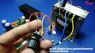
36. 1×100k single turn potentiometer.
37. 1×GBU1508 Bridge rectifier. (You can use 5A bridge rectifier)
License► ©Technical Mriganka. You can't use this Pcb Layout and Gerber File for commercial purpose. You can use this pcb layout and gerber file only for educational and diy projects.
►PCB Layout & Schematic - https://bit.ly/3ssuyzm
Specification►
R.M.S power - 100 Watts at 8Ω
Frequency Response - 30hz-20khz.
Power Supply - 33-0-33V/ 30-0-30V 5A transformer.
R.M.S power - 100 Watts at 8Ω
Frequency Response - 30hz-20khz.
Power Supply - 33-0-33V/ 30-0-30V 5A transformer.
How to make pcb by ironing method►
For make pcb you need pcb layout. download the pcb layout and print it by laser printer on photo paper. Then cut the pcb layout. Then press the pcb layout by iron on copper clad board. Press the iron 10-15 minutes. Then leave the pcb for cool down 10 minutes. when the pcb was cool, put the pcb in water and move the pcb layout to copper clad board. Then put the pcb in ferric chloride [FeCl3+H2O] for etching 10-15 minutes. when etching was end, clean the pcb by water. Then make hole on pcb. And then press the upper side print of pcb. Now your pcb is ready, mount components by instruction.
Watch This video for how to make PCB by ironing method
How to test this amplifier►
After complete this board don't forget to series light test.
After complete this board don't forget to series light test.

After connecting the series light, make sure that the series light does not turn on. If the series light not turn on, then check the voltages.

First check driver stage. Connect the black probe of multimeter on Ground, and red probe on TIP42C Collector, you get - volt (-47 to -49V). And on TIP41C Collector, you get + volt (+47 TO +49V).

Then check Biasing of this amplifier. Connect the black probe of multimeter on Ground, and red probe on TIP41C Base pin. You get = 0.5 to 0.7V

Now check OP-AMP voltage. Connect the black probe of multimeter on Ground, and red probe on UA741 ic 7 no pin, you get +volt (+15 to +16V) and on 4 no pin, you get -volt (-15 to - 16V).

Then check Speaker Output and Audio Input voltage. Here you get no voltages 0.00V.
If you get same voltages, then connect preamplifier to input and connect speaker to output.
If you get same voltages, then connect preamplifier to input and connect speaker to output.

For input you can use 100k single turn potentiometer. If you input from Stereo preamplifier, then connect two 10k 1/4w resistor in input of potentiometer.
Thank you,
Technical Mriganka.
Technical Mriganka.


0 Comments